Nvidia’s [NASDAQ: NVDA] conference last week was undoubtedly a fan-fare event.
The GPU Technology Conference, which wrapped up on Monday, was the company’s first in-person event in five years.
‘I hope you realise this is not a concert,’ Nvidia’s CEO Jensen Huang quipped to a sea of fans. But it sure felt like one.
The 900+ sessions covered the gambit from AI-drug discovery to the future of robotics.
The big spectacle was keynote speaker Jensen Huang, who captured mainstream attention by unveiling Nvidia’s new flagship platform, ‘Blackwell’.
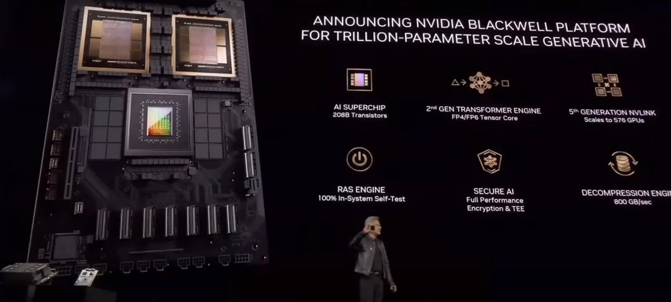
They named the platform ‘Blackwell’ after David Blackwell. He was an African American mathematician known for his work in game theory and statistics.
The ‘platform’ we’re talking about here is the host of technologies that revolve around their newest AI chip — The Blackwell AI GPU series seen above.
After its market-defining run with its previous Hopper chips, like the H100, the market eagerly awaited its latest offering.
The Blackwell GPU is planned for release in three stages. The B100, B200, and eventually the GB200.
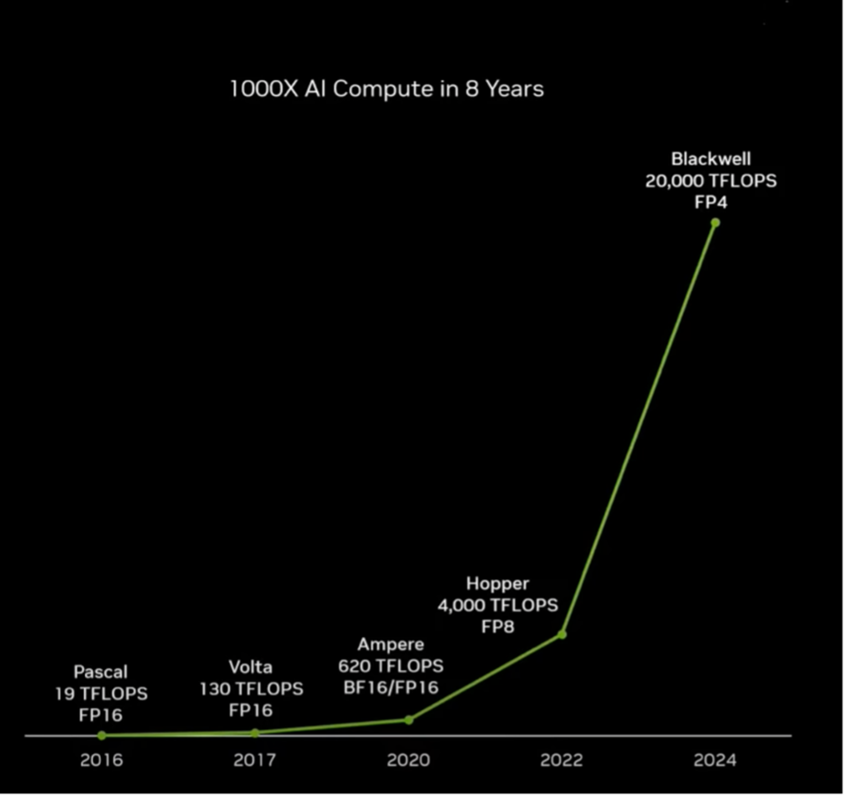
These are easily the world’s most powerful GPUs, capable of running at 20 petaFLOPS. You can think of FLOPS as a proxy for computer speed.
One petaFLOP performs one quadrillion floating point operations (calculations) per second.
If you want some kind of benchmark, your standard computer today with an Intel i7 processor operates at around 0.2 teraFLOPS.
That’s only 0.0002 petaFLOPs.
This is an impressive engineering feat, but it was by no means unexpected by serious watchers.
Regardless, charts like this were thrown around to wow the audience.
And it largely worked. As one investment newsletter wrote:
‘A five-year-old child could look at the above chart and know that something incredible just happened.’
Did it really though?
Looking around the many reports about this conference, you will likely only read lazy reports parroting specs, or how amazing these results are without context.
Now, I don’t want to be too negative. It’s clearly an impressive level of computing performance.
But what’s the catch? It turns out, there are quite a few caveats.
But that’s exciting for investors.
If market players are misinterpreting the reality of these announcements, it means that there’s hidden value in this sector.
Like all smart investments, the devil is in the details.
For starters, let’s compare the prior chart to older generations of GPUs…notice anything similar?
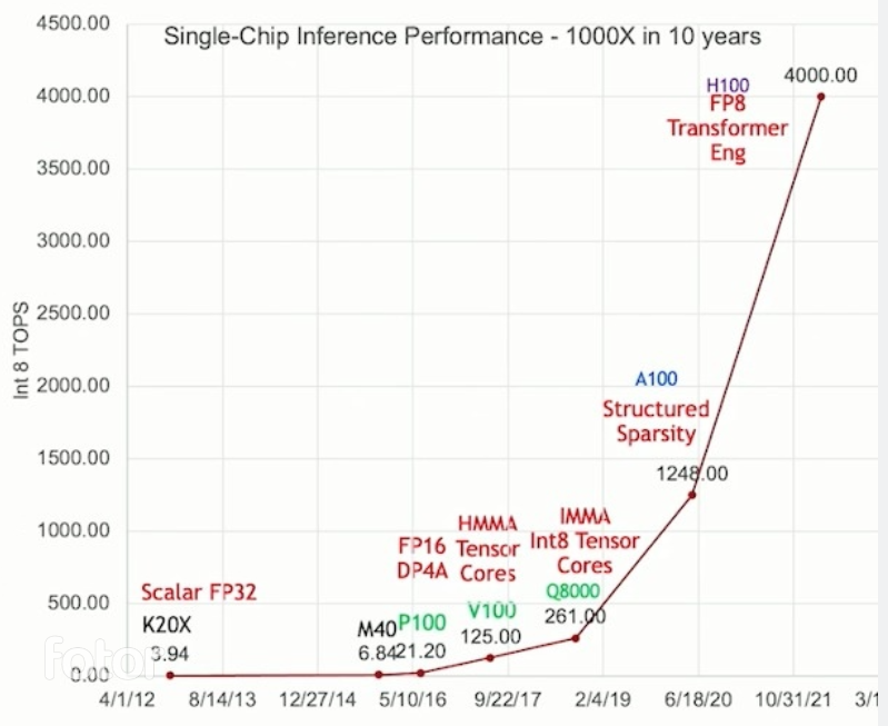
The improvements are the same!
If we went back a generation, you’d see the trend continue.
In fact, the improvements seen by the latest chip are slightly less than those seen by prior generations.
So, while it’s impressive that we continue this trend, the shift to Blackwell is not some new paradigm of power.
It’s more like business as usual for the GPU chip industry.
Interestingly, many details showed signs of Nvidia’s technical moat shrinking.
What were they?
Semiconductor’s decade-defining challenge
First, we need to go into some technical detail about semiconductor chips.
If you don’t want to dive deep into chips, that’s fine; feel free to skip to the next heading.
But I think it’s worth understanding the thing that powers the digital world around you.
I firmly believe the transistor will stand as the most significant invention of the 20th century, but what is it exactly?
Let’s use an analogy…
A transistor can be thought of as a faucet in a sink. Water flowing through the faucet is like the current flowing through the transistor.
By turning the handle of the faucet, you control the flow of water, allowing more or less to flow through.
Similarly, by applying a voltage to the base of the transistor, you can control the flow of current through the transistor.
By turning the ‘flow’ on and off, you have something that lets current flow or not.
Hence, it is a ‘semi’-conductor.
Those transistors turning on and off form the basis of the binary code (1 & 0s) that represent all the information of our digital age.
Here’s a simplified view of what these semiconductor chips look like.
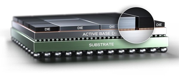
On the ‘die’ is where you’d pack those transistors and their connections (zoomed top right).
Understand this…
Those semiconductor connections are critical to performance.
Breakthroughs in speed and power often come with new generations that change these die connections and transistor shapes.
This specific area is a key battleground in the race to advance microchip technology.
Nvidia and TSMC [NASDAQ:TSM] are the major players in this field, with TSMC being the major manufacturer of Nvidia.
You can think of it as Nvidia supplying the design while TSMC makes the chip.
Nvidia’s Blackwell chip will pack an astonishing 208 billion transistors on its two combined chips.
You’ve likely heard of Moore’s Law, the idea that the number of transistors on a chip doubles every two years.
So, by 2030, we should have an astonishing 1 trillion transistors on chips.
We’ve had over 50 years of Moore’s Law, but things are starting to slow.
We’re now creating transistors that are so small that we are hitting physical barriers.
Why is this relevant to Blackwell?
Well, the Blackwell chip is the first new GPU from Nvidia that’s on the same underlying semiconductor ‘node’ or generation.
This is because Nvidia’s main chip supplier, TSMC, has had issues with its next generation of chips.
TSMC has dominated the chip space for years but is now experiencing pain as it transitions to its next nodes.
The shrinking of transistors has reached the point where their small size has caused a host of electrostatic issues on the chips.
On-chip power costs are high as transistors bleed current when not in use, parts face shrinkage, and performance improvements are slowing.
The Blackwell Chip will be one of the last FinFet transistor chips after over a decade of dominance.
What we look towards next is Gate-All-Around (GaaFET) Transistors.
PLANAR 1960S — FINFET 2010S — GATE-ALL-AROUND 2024+
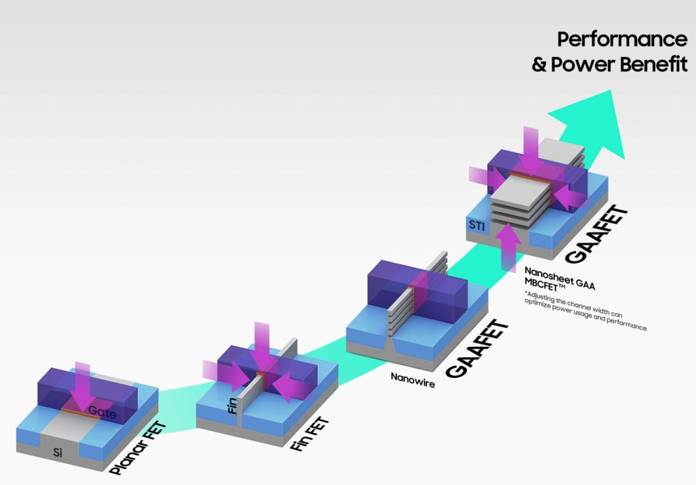
What GaaFET are is a bit complex for here, but if you want some deeper reading, then check this article out.
What is relevant to us now— and what was missed by most— is that the FinFET compromises were papered over by other specs that weren’t relevant to the GPU itself.
For example, the chip is not one GPU chip but, in fact, two that are combined. This ‘chiplet’ style has been adopted by competitors for a long time but has been historically criticised by Nvidia.
This fact was ignored by many who were instead wowed by Nvidia’s boasting of faster connection speeds between the two chips.
Other missed factors were things like the speed boasted earlier being limited to an imprecise 4-bit floating point data type and the need for liquid-cooled servers to run them.
The technical reasons for these many compromises are important to note and return to, even if you don’t understand them fully now.
Another one is known as the ‘reticle-limit’ in the world of photolithography.
This means that for future chip transistors to be smaller, they will require new specialised tools from higher up in the supply chain.
That’s from manufacturers like ASML— for their lithography machines— or Zeiss for their lenses.
In fact, if you continue up this incredibly complex supply chain, you will find at least four near-complete monopolies.
These go all the way back to a single quartz factory in North Carolina that supplies the whole sector.
From specialist chemicals in Japan to high bandwidth memory from Korea — the story is more complex than many imagine.
Here is a good overview of what the semiconductor space looks like presently.
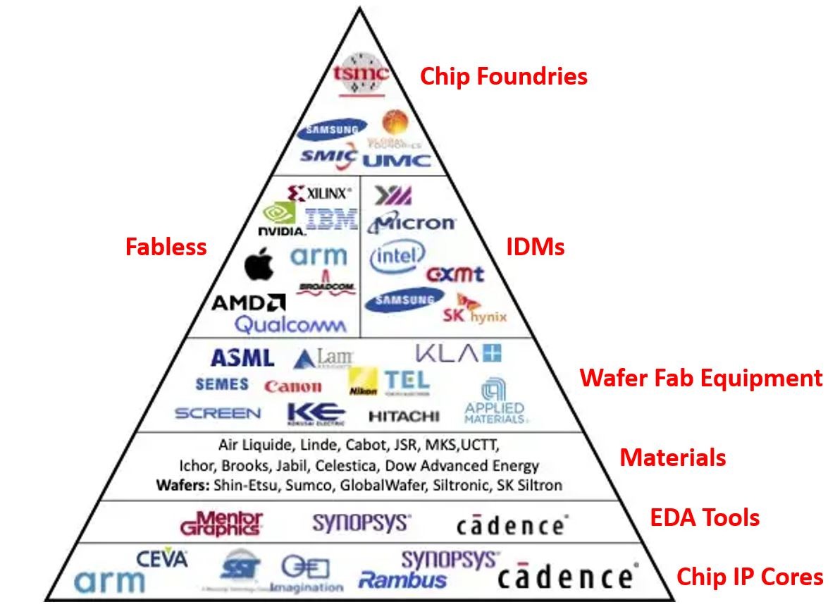
The takeaway here is that this whole supply chain is a delicate balance that crosses many countries beyond the singular focus on Taiwan.
So any big change from here will require a complex interplay of supply agreements and technological retooling that can’t be flicked like a switch.
A good example was the US-imposed export ban of ASML lithography tools that froze China out of the latest chip production.
As a response I’d anticipate the less complex chip market soon being flooded by Chinese players.
But for Nvidia…
What do these changes mean?
A new generation of chips is required beyond Nvidia’s Blackwell.
These changes require a significant shift in both chip design and the lithography tools to build them.
This means a window has opened up for competitors to regain market share in semiconductors and chips like GPUs.
TSMC and Nvidia’s main competitors have long understood this and waved the white flag long ago.
Instead of competing now, they’ve begun spending on the next generation of transistors and chips.
Samsung and IBM were the first to design these new generations of GaaFET transistors.
And while TSMC says it expects volume production to begin in 2025. Between now and then is a clear opening for disruption.
For Alpha Tech Trader members, I’ll be looking carefully at another chipmaker who I think could re-assert itself on the global stage as the premier chip marker.
But for now, it’s Nvidia and TSMCs world, and I’ll be keenly watching what these leading companies do next…
For Investors who aren’t already part of Alpha Tech Trader and want to join in the coming opportunities in tech and other sectors, we have opened the Speculators Club.
It’s not a new trading advisory but a limited-time offer on a collection of our services that are ready to seize this bull market moment.
Learn how to sign up here.
Regards,
Charlie Ormond,
Tech Analyst, Alpha Tech Trader


Comments